
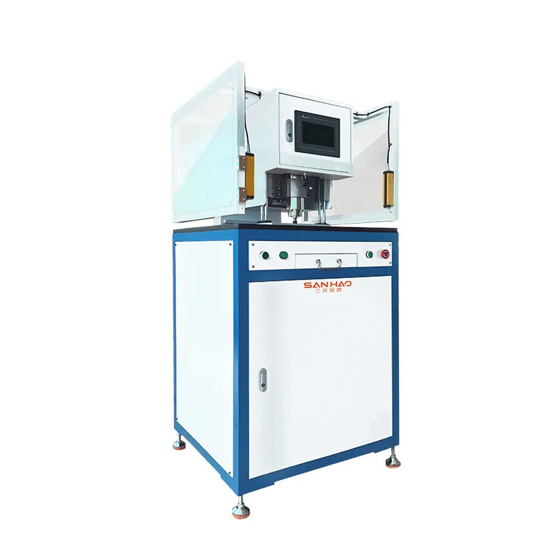
automatic sampling machine
Automatic Sampling Machine
It provides high-precision and non-destructive sample cutting for metallographic cross-section analysis of PCB (Printed Circuit Board).
产品用途
1. Specially designed for high-precision sampling of PCB metallographic cross-sections. It can rapidly cut printed boards, substrate copper foils and assembled boards to obtain standard-sized specimens for metallographic analysis.
2. Suitable for targeted sampling of finished PCBs, semi-finished products and soldered assembly boards, meeting the requirements of incoming material inspection, process monitoring and failure analysis.
3. It can perform non-destructive or minimally destructive section sampling on key areas such as through holes, blind holes, buried holes, circuit traces and solder joints, fully preserving plating layers and interfacial morphology to ensure authentic and reliable metallographic evaluation results.
立即咨询:0755-27207716