
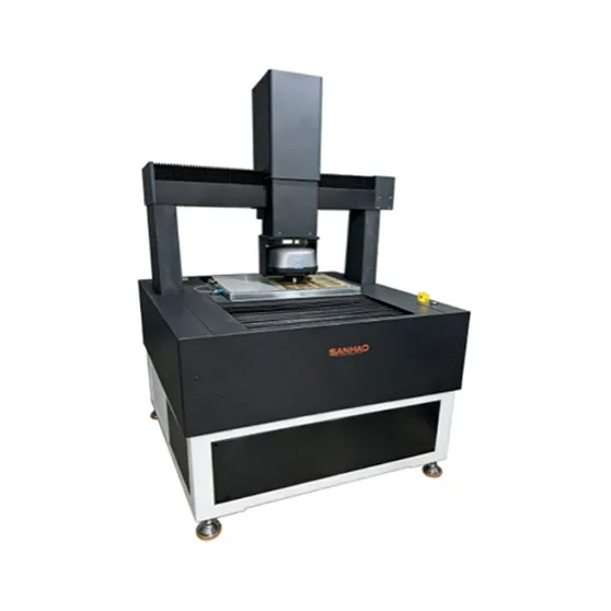
1. Adopting dual measurement principles of laser confocal and focal variation, the instrument can measure highly reflective metal surfaces such as copper foils and pads, as well as low-reflective non-metallic areas including solder mask and substrate, fulfilling micro-morphology analysis requirements for all types of PCB materials.
2. Equipped with a 661nm semiconductor laser light source, it causes minimal damage to photoresists and organic materials while delivering excellent depth resolution, applicable for measuring PCB blind holes, through holes, circuit steps and plating thickness.
3. An ultra-fine color CMOS sensor serves as the white light receiver, enabling simultaneous color image capture during laser measurement to facilitate identification of PCB surface defects such as oxidation, contamination, solder mask bubbles and circuit scratches.
4. A 6-position motorized objective turret enables automatic objective switching; low-magnification positioning and high-precision measurement can be completed with one click. Combined with motorized focusing, it supports multi-magnification sequential scanning and depth fusion, boosting efficiency for PCB cross-section analysis and batch inspection.
5. Motorized focusing features nanometer-level stepping precision with fast and stable auto-focusing, eliminating manual focusing errors and ensuring excellent measurement repeatability, ideal for precise focusing on fine circuits, blind hole bottoms and multi-layer board cross-sections.
6. X/Y/Z axes support dual control via software and joystick. The joystick enables rapid manual sample positioning, while the software supports programmable automatic grid scanning and fixed-point return, balancing flexibility and automation to accommodate R&D sampling inspection and mass production line testing scenarios.